Payment Terms :T/T, Western Union, Paypal, Trade Assurance, Credit Card
Supply Ability :328 pcs
Delivery Time :3-5 Day
Packaging Details :International Standard Packaging
Category :Programmable Logic ICs
Condition :Original 100%,Brand New and Original,New
Number of I/Os :680 I/O
Product :Virtex-5
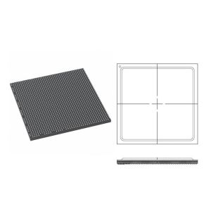
Package / Case :FCBGA-1738
Distributed RAM :1240 kbit
Embedded Block RAM - EBR :8208 kbit
Data Rate :6.5 Gb/s
Service :BOM Kitting
Lead time :In Stock,contact us
more
Contact Now
Add to Cart
Find Similar Videos
View Product Description
XC5VFX100T-1FF1738C IC FPGA FCBGA-1738 Field Programmable Gate Array
Product Attribute
Attribute Value
Xilinx
FPGA - Field Programmable Gate Array
Virtex-5
680 I/O
1 V
0 C
+ 85 C
SMD/SMT
FCBGA-1738
Data Rate:
6.5 Gb/s
Series:
XC5VFX100T
Brand:
Xilinx
Distributed RAM:
1240 kbit
Embedded Block RAM - EBR:
8208 kbit
Maximum Operating Frequency:
550 MHz
Moisture Sensitive:
Yes
Number of Transceivers:
16 Transceiver
Product Type:
FPGA - Field Programmable Gate Array
Factory Pack Quantity:
1
Subcategory:
Programmable Logic ICs
Tradename:
Virtex
Summary of Virtex-5 FPGA Features
• Five platforms LX, LXT, SXT, TXT, and FXT − Virtex-5 LX: High-performance general logic applications − Virtex-5 LXT: High-performance logic with advanced serial connectivity − Virtex-5 SXT: High-performance signal processing applications with advanced serial connectivity − Virtex-5 TXT: High-performance systems with double density advanced serial connectivity − Virtex-5 FXT: High-performance embedded systems with advanced serial connectivity
• Cross-platform compatibility − LXT, SXT, and FXT devices are footprint compatible in the same package using adjustable voltage regulators
• Most advanced, high-performance, optimal-utilization, FPGA fabric − Real 6-input look-up table (LUT) technology − Dual 5-LUT option − Improved reduced-hop routing − 64-bit distributed RAM option − SRL32/Dual SRL16 option • Powerful clock management tile (CMT) clocking − Digital Clock Manager (DCM) blocks for zero delay buffering, frequency synthesis, and clock phase shifting − PLL blocks for input jitter filtering, zero delay buffering, frequency synthesis, and phase-matched clock division